Google’s TPU 8tx and 8i Max are split for a reason: security on one side, memory pressure on the other
Google’s new TPUs target different jobs: confidential inference on 8tx and long-context, memory-heavy workloads on 8i Max.
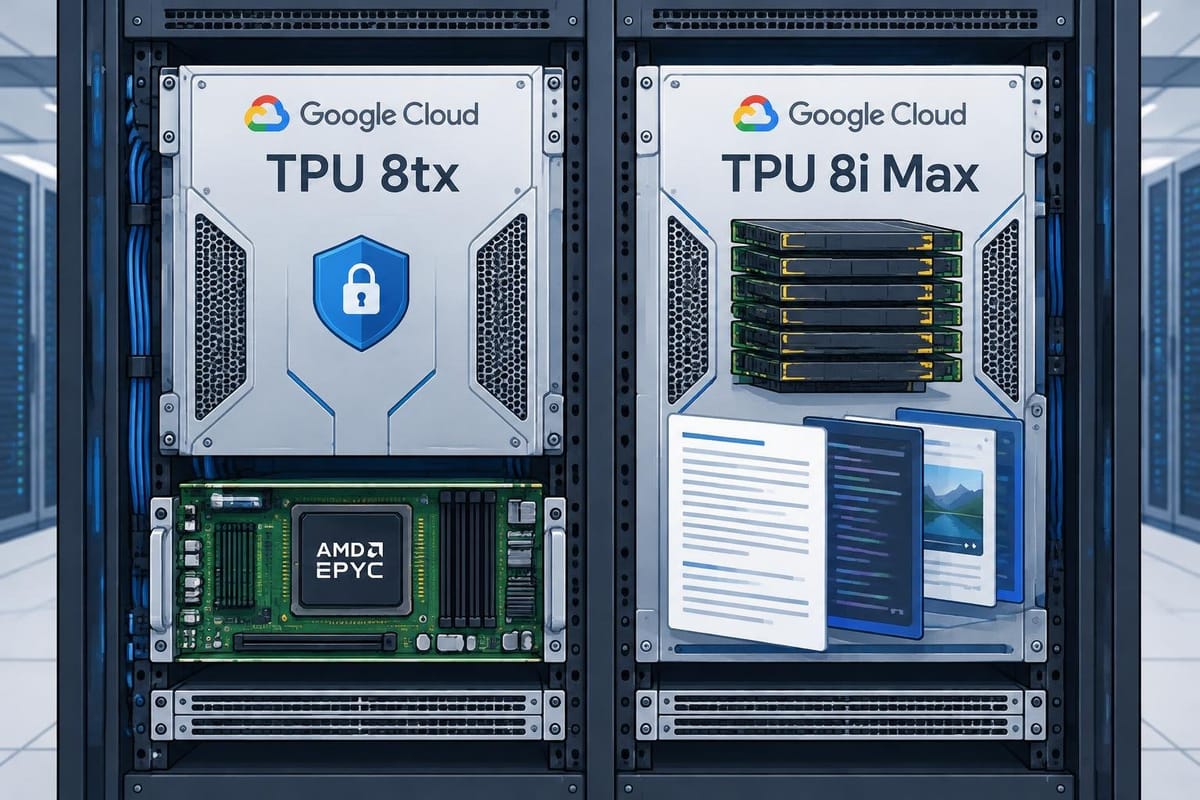
Google’s new TPU pair is less a single chip race with Nvidia than a sign that the company is carving AI hardware into narrower jobs.
In its Nov. 9 announcement, Google said it expanded its eighth-generation TPU portfolio with TPU 8tx for secure, confidential inference and TPU 8i Max for massive context windows. The company said the additions bring the generation to four systems in a single year, and that the new designs are meant to support different parts of the AI lifecycle, from training and serving to agentic workloads. [Source: https://blog.google/innovation-and-ai/infrastructure-and-cloud/global-network/tpu-8i-max-and-8tx/]
That split matters because it tells buyers what Google thinks is now limiting AI systems most: for one class of workloads, the bottleneck is security and regulated-data handling; for the other, it is memory bandwidth and the ability to keep long-running context alive.
What Google says each system is for
Google’s own framing is the clearest guide.
- TPU 8tx: secure, confidential inference; also described by Google as useful for small-scale training. [Source: https://blog.google/innovation-and-ai/infrastructure-and-cloud/global-network/tpu-8i-max-and-8tx/]
- TPU 8i Max: massive context windows and the highest compute density per rack. [Source: https://blog.google/innovation-and-ai/infrastructure-and-cloud/global-network/tpu-8i-max-and-8tx/]
Bloomberg’s reporting matched that split: 8tx is aimed at secure, confidential work, while 8i Max is intended for AI applications that require long-context windows. The same report said Google is adding these as reconfigured versions of existing TPU systems rather than all-new silicon. [Source: https://finance.yahoo.com/technology/ai/articles/google-escalates-nvidia-rivalry-specialized-123000247.html]
That is the core of the story. Google is not presenting one universal accelerator as a better Nvidia alternative. It is presenting a portfolio of systems, each tuned to a workload class customers have been asking for.
TPU 8tx: confidential inference, not just faster inference
Google says TPU 8tx is based on the same silicon as TPU 8t and is paired with 5th Generation AMD EPYC CPU hosts. The company says it adds hardware-level confidential compute so sensitive data and model weights remain protected and isolated even while in use. Google also says 8tx uses the same low-latency Boardfly network it built for real-time reasoning, and claims up to 2x lower latency versus TPU 8t with a near-zero performance penalty. [Source: https://blog.google/innovation-and-ai/infrastructure-and-cloud/global-network/tpu-8i-max-and-8tx/]
That makes 8tx look like more than a performance refresh. It is a system built for regulated enterprises and governments that want to run models and autonomous agents close to private data without moving that data between clusters. Google says the system can support private fine-tuning, model distillation, and reinforcement learning on one configuration. [Source: https://blog.google/innovation-and-ai/infrastructure-and-cloud/global-network/tpu-8i-max-and-8tx/]
Chosun Biz reported the same broad picture and added that Google Cloud worked with AMD to apply encryption across the CPU-to-TPU data path and on the chip and memory. It also said 8tx is the first Google TPU to support confidential computing and that the company claimed inference latency was cut by up to half versus TPU 8t. [Source: https://biz.chosun.com/en/en-it/2026/11/09/ZLZV3H4TYNC5LM5XL57F2EPZ7Y/]
The practical implication: 8tx is not just for fast serving. It is for customers whose first question is whether the accelerator can be trusted with live prompts, model weights and regulated data.
TPU 8i Max: a memory product in accelerator form
Google’s description of TPU 8i Max is even more explicit about the bottleneck it is addressing.
The company says 8i Max combines two low-latency TPU 8i chips into a single package. Google says that doubles compute, SRAM and HBM bandwidth versus TPU 8i. It describes the system as being built for “massive context windows,” and says it offers the highest compute density per rack. [Source: https://blog.google/innovation-and-ai/infrastructure-and-cloud/global-network/tpu-8i-max-and-8tx/]
Google says the reason for that packaging choice is simple: when dozens of AI agents work across a codebase or hours of video, memory bandwidth quickly becomes the bottleneck. [Source: https://blog.google/innovation-and-ai/infrastructure-and-cloud/global-network/tpu-8i-max-and-8tx/]
Chosun Biz reported the most concrete specifications in the launch material: 384 GB of HBM, up 33% from TPU 8i; 17.2 TB/s of bandwidth, or 2x the previous level; and 768 MB of on-chip SRAM, also doubled. [Source: https://biz.chosun.com/en/en-it/2026/11/09/ZLZV3H4TYNC5LM5XL57F2EPZ7Y/]
That makes 8i Max look less like a pure compute upgrade and more like a bandwidth-and-capacity product. If the model or agent is stalling because it cannot hold enough context or move it fast enough, more arithmetic alone does not solve the problem. Google is trying to solve the memory wall at the system level.
Why Google is splitting the lineup
Google’s announcement is also a statement about how it wants to compete. In the blog post, the company said its eighth-generation systems now target distinct stages of the AI lifecycle and that its approach is to build “the computer around the chip,” adjusting packaging, memory, networking and security around a shared silicon base. [Source: https://blog.google/innovation-and-ai/infrastructure-and-cloud/global-network/tpu-8i-max-and-8tx/]
That points to three things Google appears to be optimizing for:
- Confidential computing for regulated and private enterprise workloads.
- Long-context inference where memory capacity and bandwidth matter as much as peak compute.
- System-level efficiency, where the host CPU, network fabric and software stack are tuned around the TPU rather than treated as afterthoughts.
Google is also trying to improve utilization. It announced TPU Sync, an open-source model-state layer that moves working memory off the TPU when an agent pauses and restores it later. Google says that can cut KV transfer latency and time to first token by more than 90% in its own framing, which is a sign that the company sees accelerator idle time as an economic problem as much as a technical one. [Source: https://blog.google/innovation-and-ai/infrastructure-and-cloud/global-network/tpu-8i-max-and-8tx/]
The company did not publish a direct cost-per-token comparison for 8tx or 8i Max in the announcement, so any cost story has to be read from those utilization and memory-efficiency claims rather than from a posted price sheet.
What is confirmed, and what is inference
Confirmed from Google’s announcement:
- TPU 8tx and TPU 8i Max are new eighth-generation TPU systems. [Source
- 8tx is for secure, confidential inference and is also described as useful for small-scale training. [Source: https://blog.google/innovation-and-ai/infrastructure-and-cloud/global-network/tpu-8i-max-and-8tx/]
- 8tx uses 5th Generation AMD EPYC CPU hosts and the Boardfly network. [Source
- 8i Max is for massive context windows and combines two TPU 8i chips in one package. [Source: https://blog.google/innovation-and-ai/infrastructure-and-cloud/global-network/tpu-8i-max-and-8tx/]
- Google says 8i Max doubles compute, SRAM and HBM bandwidth versus TPU 8i. [Source: https://blog.google/innovation-and-ai/infrastructure-and-cloud/global-network/tpu-8i-max-and-8tx/]
- Google says TPU Sync is meant to raise utilization and reduce infrastructure cost through better memory movement. [Source: https://blog.google/innovation-and-ai/infrastructure-and-cloud/global-network/tpu-8i-max-and-8tx/]
Reasonable inference from those details:
- 8tx is aimed at customers that need confidential inference without separating sensitive data across multiple clusters.
- 8i Max is aimed at agentic, long-context workloads where memory bandwidth is the limiting factor.
- Google’s segmentation is about system economics, not just headline chip speed.
What the sources do not fully provide:
- No public list price for either system.
- No independent benchmark data in the source materials available here.
- No exact general-availability date in the announcement itself.
The bigger signal
The broader message is that Google is moving away from the idea that one TPU design should cover every AI workload. Instead, it is offering purpose-built systems for secure inference, training, reasoning and long-context processing.
For buyers, that means the relevant question is not which TPU is “faster” in the abstract. It is which system matches the workload.
If you are running regulated enterprise inference, 8tx is the relevant system. If you are running agents over long context windows, codebases or video, 8i Max is the one that matters.
That is a more specific and more useful story than a generic chip rivalry frame. Google is signaling that AI infrastructure is fragmenting along the same lines as the workloads themselves: security, memory, and context length.

Comments ()